Laser slicing will become the mainstream technology for cutting 8-inch silicon carbide in the future
Q: What are the main technologies for silicon carbide slicing processing?
A: The hardness of silicon carbide is second only to that of diamond, and it is a high-hardness and brittle material. The process of cutting the grown crystals into sheets takes a long time and is prone to cracking. As the first process in the processing of silicon carbide single crystals, the performance of slicing determines the subsequent grinding, polishing, thinning and other processing levels. Slicing processing is prone to cause cracks on the surface and subsurface of the wafer, increasing the breakage rate and manufacturing cost of the wafer. Therefore, controlling the surface crack damage of the wafer slicing is of great significance for promoting the development of silicon carbide device manufacturing technology. The currently reported silicon carbide slicing processing technologies mainly include consolidation, free abrasive slicing, laser cutting, cold separation and electrical discharge slicing, among which reciprocating diamond consolidated abrasive multi-wire cutting is the most commonly used method for processing silicon carbide single crystals. When the size of the crystal ingot reaches 8 inches or more, the requirements for wire cutting equipment are very high, the cost is also very high, and the efficiency is too low. There is an urgent need to develop new cutting technologies that are low-cost, low-loss and high-efficiency.
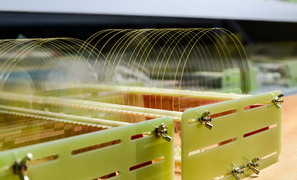
ZMSH's SiC crystal ingot
Q: What are the advantages of laser slicing technology over traditional multi-wire cutting technology?
A: In the traditional wire cutting process, silicon carbide ingots need to be cut along a certain direction into thin sheets with a thickness of several hundred microns. These sheets are then ground with diamond grinding fluid to remove tool marks and surface subsurface crack damage and reach the required thickness. After that, CMP polishing is carried out to achieve global planarization, and finally, the silicon carbide wafers are cleaned. Due to the fact that silicon carbide is a high-hardness and brittle material, it is prone to warping and cracking during cutting, grinding and polishing, which increases the breakage rate of the wafer and the manufacturing cost. Moreover, the surface and interface roughness is high, and the pollution is severe (such as dust and wastewater). Additionally, the multi-wire cutting processing cycle is long and the yield is low. It is estimated that the traditional multi-wire cutting method has an overall material utilization rate of only 50%, while after polishing and grinding, the cutting loss ratio is as high as 75%. Early production statistics from abroad show that with 24-hour continuous parallel production, it takes about 273 days to produce 10,000 pieces, which is a relatively long time.
At present, most domestic silicon carbide crystal growth enterprises adopt the approach of "how to increase production" and significantly raise the number of crystal growth furnaces. In fact, when the crystal growth technology is not yet fully mature and the yield rate is relatively low, they should consider "how to save" more. The adoption of laser slicing equipment can significantly reduce losses and increase production efficiency. According to estimates, taking a single 20-millimeter SiC ingot as an example, 30 350um wafers can be produced using a wire saw, while more than 50 wafers can be produced with laser slicing technology. Meanwhile, due to the better geometric characteristics of the wafers produced by laser slicing, the thickness of a single wafer can be reduced to 200um, which further increases the number of wafers. A single 20mm SiC ingot can produce over 80 wafers. The traditional multi-wire cutting technology has been widely applied in silicon carbide of 6 inches and below. However, it takes 10 to 15 days to cut 8-inch silicon carbide, which has high requirements for equipment, high cost and low efficiency. Under such circumstances, the technical advantages of large-sized laser slicing become apparent and it will become the mainstream technology for 8-inch cutting in the future. Laser cutting of 8-inch silicon carbide ingots can achieve a single-piece cutting time of less than 20 minutes per piece, while the single-piece cutting loss is controlled within 60um.
ZMSH's SiC crystal ingot
Overall, compared with multi-wire cutting technology, laser slicing technology has advantages such as high efficiency and speed, high slicing rate, low material loss, and cleanliness.
Q: What are the main difficulties in silicon carbide laser cutting technology?
A: The main process of silicon carbide laser cutting technology consists of two steps: laser modification and wafer separation.
The core of laser modification is to shape and optimize the laser beam. Various parameters such as laser power, spot diameter, and scanning speed will all affect the effect of silicon carbide ablation modification and subsequent wafer separation. The geometric dimensions of the modification zone determine the surface roughness and the subsequent separation difficulty. High surface roughness will increase the difficulty of subsequent grinding and increase material loss.
After laser modification, the separation of wafers mainly relies on shear force to peel the cut wafers off the ingots, such as cold cracking and mechanical tensile force. Currently, domestic manufacturers' research and development mostly use ultrasonic transducers to separate by vibration, which may lead to problems such as fragmentation and chipping, thereby reducing the yield of finished products.
The above two steps should not pose significant difficulties for most research and development units. However, due to the different processes and doping of crystal ingots from various crystal growth manufacturers, the quality of crystal ingots varies greatly. Or, if the internal doping and stress of a single crystal ingot are uneven, it will increase the difficulty of crystal ingot slicing, increase losses and reduce the yield of finished products. Merely identifying through various detection methods and then conducting zonal laser scanning slicing may not have a significant effect on improving efficiency and slice quality. How to develop innovative methods and technologies, optimize the slicing process parameters, and develop laser slicing equipment and technologies with universal processes for crystal ingots of different qualities from different manufacturers is the core of large-scale application.
Q: Besides silicon carbide, can laser slicing technology be applied to the cutting of other semiconductor materials?
A: Early laser cutting technology was applied in various material fields. In the semiconductor field, it was mainly used for dicing chip wafers. Currently, it has expanded to the slicing of large-sized single crystals. In addition to silicon carbide, it can also be used for slicing high-hardness or brittle materials such as single crystal materials like diamond, gallium nitride and gallium oxide. The team from Nanjing University has done a lot of preliminary work on the slicing of these several semiconductor single crystals, verifying the feasibility and advantages of the laser slicing technology for semiconductor single crystals.
ZMSH's Diamond wafer & GaN wafer
Q: Are there any mature laser slicing equipment products in our country at present? What stage are you currently at in the research and development of this device?
A: Large-sized silicon carbide laser slicing equipment is regarded by the industry as the core equipment for slicing 8-inch silicon carbide ingots in the future. Large-sized silicon carbide ingot laser slicing equipment can only be provided by Japan. It is expensive and subject to an embargo against China. According to research, the domestic demand for laser slicing/thinning equipment is estimated to reach around 1,000 units based on the number of wire cutting units and the planned capacity of silicon carbide. Currently, domestic companies such as Han's Laser, Delong Laser, and Jiangsu General have invested huge amounts of money in developing related products, but no mature domestic commercial equipment has yet been applied in production lines.
As early as 2001, the team led by Academician Zhang Rong and Professor Xiu Xiangqian from Nanjing University developed a laser exfoliation technology for gallium nitride substrates with independent intellectual property rights, accumulating a rich research foundation. In the past year, we have applied this technology to the laser cutting and thinning of large-sized silicon carbide. We have completed the development of prototype equipment and slicing process research and development, achieving the cutting and thinning of 4-6 inch semi-insulating silicon carbide wafers and the slicing of 6-8 inch conductive silicon carbide ingots. The slicing time for 6-8-inch semi-insulating silicon carbide is 10-15 minutes per slice, with a single-slice loss of less than 30 μ m. The single-piece cutting time for 6-8-inch conductive silicon carbide ingots is 14-20 minutes per piece, with a single-piece loss of less than 60um. It is estimated that the production rate can be increased by more than 50%. After slicing and grinding and polishing, the geometric parameters of the silicon carbide wafers comply with the national standards. The research results also show that the thermal effect during laser slicing has no significant influence on the stress and geometric parameters of silicon carbide. Using this equipment, we also conducted a feasibility verification study on the slicing technology of single crystals of diamond, gallium nitride and gallium oxide.
As an innovative leader in silicon carbide wafer processing technology, ZMSH has taken the lead in mastering the core technology of 8-inch silicon carbide laser slicing. Through its independently developed high-precision laser modulation system and intelligent thermal management technology, it has successfully achieved an industry breakthrough by increasing the cutting speed by more than 50% and reducing material loss to within 100μm. Our laser slicing solution employs ultraviolet ultra-short pulse lasers in combination with an adaptive optical system, which can precisely control the cutting depth and heat-affected zone, ensuring that the TTV of the wafer is controlled within 5μm and the dislocation density is less than 10³cm⁻², providing reliable technical support for the large-scale mass production of 8-inch silicon carbide substrates. At present, this technology has passed automotive-grade verification and is being applied industrially in the fields of new energy and 5G communication.
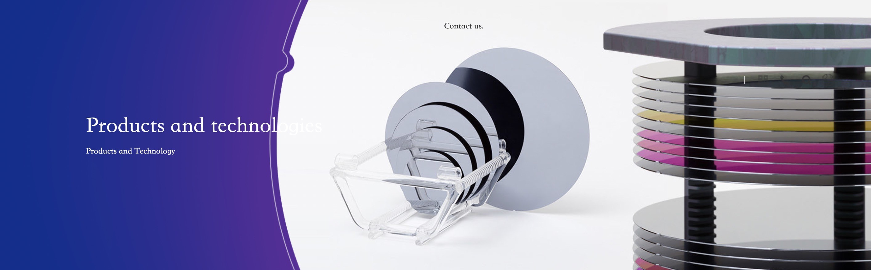
The following is the SiC 4H-N & SEMI type of ZMSH:
* Please contact us for any copyright concerns, and we will promptly address them.

 Your message must be between 20-3,000 characters!